Netlist for Z80 with FlashRAM, static RAM and a UART
This is a netlist for my current board as of November 2013, which includes:- A 6mHz Z80 (slow clocked)
- Arduino providing variable clock (ugh)
- 1Mbit FlashRAM providing 32k of ROM
- 32k Static RAM
- 7400 NAND doing memory decoding
- 16mHz oscillator for the...
- 16C550 UART
- MAX232 doing TTL to RS232 level conversions
NAND as a memory decoder, splitting the memory space in half between a lower 32k of ROM ($0000 to $7fff) and upper 32k of RAM ($8000 to $ffff). The only purpose the 7400
serves on this board is to do this memory decoding.
The UART is providing a simple serial terminal, so none of the fancier signals like DTR/CTS/etc are being used. The UART operates at TTL voltages, but RS232 operates at a
wider range, so a MAX232 is utilised to get it to the right voltage ranges.
The netlist tables will provide the chip, the pin number, the signal name and what it is connected to. The format of the 'connect to' field indicates which device the
pin is connected to, the signal name on that device and the associated pin number. Remember, if a signal begins with a '/' it indicates that the signal
is active low. If a pin is connected to more than one device, or pin, they are separates by commas.
So, "UART /IOW/18, RAM /WE/27" indicates that this pin is connected to the UART, signal /IOW (active low) which is pin 18 on that device, as well as the RAM, signal /WE
(active low), which is pin 27 on that device.
| Pin | Signal | Connected to |
| Z80 | ||
| 27 | /M1 | N/C |
| 19 | /MREQ | 7400 AIn0/1, 7400 AIn1/2 |
| 20 | /IORQ | UART /CS2/14 |
| 21 | /RD | UART /IOR/21, Flash /OE/24, RAM /OE/22 |
| 22 | /WR | UART /IOW/18, RAM /WE/27 |
| 28 | /RFSH | N/C |
| 18 | /HALT | N/C |
| 24 | /WAIT | Tied to Vcc |
| 16 | /INT | Tied to Vcc |
| 17 | /NMI | Tied to Vcc |
| 26 | /RESET | 740 Ohm resistor tied Vcc, Intermittant button to GND |
| 25 | /BUSRQ | Tied to Vcc |
| 23 | /BUSACK | N/C |
| 6 | CLK | Clock (Arduino) |
| 11 | +5v | Vcc |
| 29 | GND | GND |
| 30,31,32,33,34,35,36,37,38,39,40,1,2,3,4,5 | A0-A15 | Address bus |
| 14,15,12,8,7,9,10,13 | D0-D7 | Data bus |
| FlashRAM | ||
| 1 | Vpp | N/C |
| 31 | /PGM | N/C |
| 30 | N/C | N/C |
| 24 | /OE | Z80 /RD/21 |
| 22 | /CE | 7400/8 |
| 16 | GND | GND |
| 32 | Vcc | Vcc |
| 2 | A16 | N/C |
| 12,11,10,9,8,7,6,5,27,26,23,25,4,28,29,3 | A0-A15 | Address bus |
| 13,14,15,17,18,19,20,21 | D0-D7 | Data bus |
| Static RAM | ||
| 20 | /CS | 7400 DOut/11 |
| 22 | /OE | Z80 /RD/21 |
| 27 | /we | z80 /WR/22 |
| 28 | Vcc | Vcc |
| 14 | GND | GND |
| 10,9,8,7,6,5,4,3,25,24,21,23,2,26,1 | A0-A14 | Address bus |
| 11,12,13,15,16,17,18,19 | D0-D7 | Data bus |
| 7400 | ||
| 1 | AIn0 | Z80 /MREQ/19 |
| 2 | AIn1 | Z80 /MREQ/19 |
| 3 | AOut | 7400 DIn1/13, 7400 CIn1/10 |
| 4 | BIn0 | N/C |
| 5 | BIn1 | N/C |
| 6 | BOut | N/C |
| 7 | GND | GND |
| 8 | COut | Flash /CE/22 |
| 9 | CIn2 | 7400 DOut/11 |
| 10 | CIn1 | 7400 AOut/3 |
| 11 | DOut | RAM /CS/20, 7400 CIn2/9 |
| 12 | DIn2 | Z80 A15/5 |
| 13 | DIn1 | 7400 AOut/3 |
| 14 | Vcc | Vcc |
| UART | ||
| 1,2,3,4,5,6,7,8 | D0-D7 | Data bus |
| 28,27,26 | A0-A2 | Address bus |
| 9 | RCLK | UART /BADOUT/15 |
| 10 | RX | MAX232 R1Out/12 |
| 11 | TX | MAX232 T1In/11 |
| 12 | CS0 | 740 Ohm resistor Tied to Vcc |
| 13 | CS1 | 740 Ohm resistor Tied to Vcc |
| 14 | /CS2 | Z80 /IORQ/20 |
| 15 | /BAUDOUT | UART RCLK/9 |
| 16 | XTAL1 | Oscillator/3 |
| 17 | XTAL2 | N/C |
| 18 | /IOW | Z80 /WR/22 |
| 19 | IOW | Tied to GND |
| 20 | GND | GND |
| 21 | /IOR | Z80 /RD/21 |
| 22 | IOR | Tied to GND |
| 23 | /DDIS | Tied to GND |
| 24 | /TXRDY | N/C |
| 25 | /AS | N/C |
| 29 | /RXRDY | N/C |
| 30 | INT | N/C |
| 31 | /OUT2 | LED (Yellow) |
| 32 | /RTS | N/C |
| 33 | /DTR | N/C |
| 34 | /OUT1 | LED (Red) |
| 35 | RESET | Flying wire (manual pull high for RESET) |
| 36 | /CTS | N/C |
| 37 | /DSR | N/C |
| 38 | /DCD | N/C |
| 39 | /RI | N/C |
| 40 | Vcc | Vcc |
| Oscillator | ||
| 1 | N/C | N/C |
| 2 | Vcc | Vcc |
| 3 | Output | UART XTAL1/16 |
| 4 | GND | GND |
| MAX232 | ||
| 1 | C1+ | +side of 1uF cap to M232/3 |
| 2 | Vs+ | +side of 1uF cap to Vcc |
| 3 | C1- | -side of 1uF cap to M232/1 |
| 4 | C2+ | +side of 1uF cap to M232/5 |
| 5 | C2- | -side of 1uF cap to M232/4 |
| 6 | Vs- | -side of 1uF cap to GND |
| 7 | T2Out | N/C |
| 8 | R2In | N/C |
| 9 | R2Out | N/C |
| 10 | T2In | N/C |
| 11 | T1In | UART Tx/11 |
| 12 | R1Out | UART RX/10 |
| 13 | R1In | DB9/Pin 3 |
| 14 | T1Out | DB9/Pin 2 |
| 15 | GND | GND, DB9/Pin 1 |
| 16 | Vcc | Vcc |
- All of the caps on the MAX232 are for the chargepumps that convert the TTL voltages (0 to +5v) to the wider RS232 voltages (-8v to +12v). It's looks like a mess, but it's right.
- I have 1uF decoupling caps between GND and Vcc on all devices (decoupling caps smooth the voltage in the circuit, reducing the possibilities of oddities due to dirty voltage.)
- The circuit requires a +5v (DC) power supply - I made my own from a 9vDC wallwart and a 7805 voltage regulator.
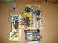
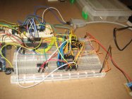
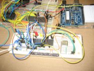
Pictures:
 |
 |
 |
| Med [625k] Large [3.1M] | Med [625k] Large [3.1M] | Med [625k] Large [3.1M] |